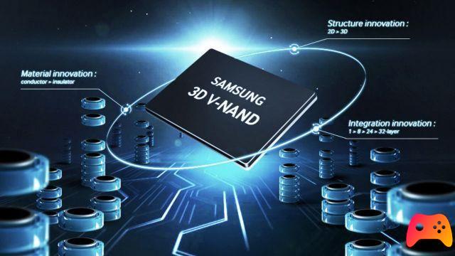
Samsung Electronics is reportedly developing its memory V-NAND of the seventh generation with ultra-high 3D stacking. The first model will present at least 160 levels, later models will offer more. Samsung, which never wanted to hand over the technology initiative to the Chinese YMTC, is expected to launch the first 160-layer V-NAND in the period in which the 3-layer 128D NAND flash of YMTC will reach mass production towards the end of 2020.

The heart of the ultra-high 3D stack is proprietary technology Double Stack by Samsung. Double stack technology creates electron holes in two separate times for current to pass through the circuits. Current generation single-stack chips create these holes once for the entire stack of the cycle. The 160-layer NAND flash is expected to announce a 67% increase in densities per package over 96-layer chips on the market. Densities could also be increased by other means, such as moving to new semiconductor fabrication nodes and PLC (5 bits per cell), currently under development by KIOXIA.